Product
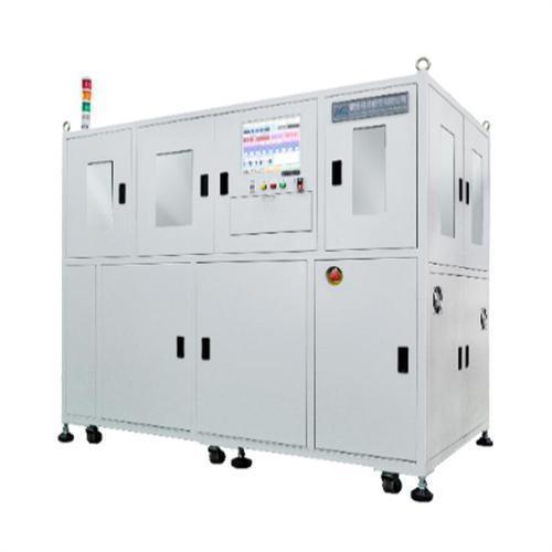
NEMST-2002IL 系列
In-line Plasma Cleaner (Fully In-line)
- Full In-line Plasma, Connecting to Upstream and Downstream Tools.
- Advanced Flow Pattern Design.
- High-Speed Plasma Cleaning: 28~33 seconds/cycle in general, including loading, plasma treatment, and unloading.
- Low-Temperature Plasma Cleaning.
- Chamber Capability: 1~2 strips of subWholestrates or lead-frames in one cycle. Operation Mode: Manual or Auto Mode.
- High Automation and Operation Friendly Design.
- Connecting with upstream and downstream tools. Multiple Processing Gases (Ar, O2, H2, mixed gas, etc.) can achieve the best surface cleaning and treatment effects. Physical, Chemical, or Physical/Chemical Mode Cleaning Method. Extremely High Cleaning Uniformity. Very Little Gas Consumption.
- Apply to Process before Die-bonding, Wire-bonding or Molding in IC Packaging or LED Packaging Applications.
- Wafer Cleaning.
- Suitable for Flip-Chip, PBGA, Window-BGA, Mini-BGA, Micro-BGA, QFN/MLP, TFBGA (Film-BGA), LFBGA, VBGA (EBGA), Pin BGA, QFN/MLP, TCP, PCB, COB, Cu L/F, Ag-Plating L/F, Fe L/F, MMC, SD, Micro-SD, etc. Suitable for Surface Treatment (Cleaning, Modification) for Electronics or Non-electronics Devices/Components.